Fetch the right card
The program counter, or PC, is a byte address. It selects four loaded instruction bytes. The instruction register holds the word assembled from them.
Write a tiny real assembly program, watch values move through a processor’s logical parts, and stop at the instant an answer becomes stored state.
Enable JavaScript to change the conditions and run the interactive experiment.
An instruction selects an operation. Registers supply values, addresses select memory, and control chooses what happens next. Calculating an answer and committing it are different events in this teaching machine.
After Calculate for ADD x3,x1,x2 with x1=7, x2=5 and x3 initially 0, what is true?
The answer exists internally, but this serial model writes architectural x3 only at Commit.
The program counter, or PC, is a byte address. It selects four loaded instruction bytes. The instruction register holds the word assembled from them.
The decoder reads the instruction’s fields. An ADD chooses two register values; an immediate instruction also contains a signed constant. A destination that is also a source is read before its replacement is committed.
An arithmetic logic unit, or ALU, computes a result or an effective memory address. At the 7 + 5 checkpoint, the pending result is 12 but x3 is still 0.
LW loads a four-byte word from its computed address. SW prepares four bytes for a store. An arithmetic-only instruction has no data-memory access in its Memory phase.
Our serial teaching machine updates architectural registers or data memory, the PC and the retired-instruction count together. You can restore an earlier recorded snapshot; this does not make a real processor run backward.
Ordinary instructions advance by four bytes. A taken branch adds its signed offset to the executing instruction’s PC. JAL also saves PC + 4 in its chosen destination, unless that destination is x0.
Change 7 and 5 to 9 and 4 and predict 13. Replace ADD with SUB and predict 5. Then run the guarded sum loop at N = 3: its stored result is 6 after 13 retired instructions.
The eight supported operations are ADDI, ADD, SUB, LW, SW, BEQ, BNE and JAL from RV32I version 2.1. This is not the complete instruction set, a certified implementation or a simulator of a named commercial processor.
Each register holds 32 bits. ADD and SUB keep the low 32 result bits; these instructions do not generate an arithmetic-overflow trap. 0x80000000 is 2147483648 unsigned and −2147483648 signed. Changing the display does not change the stored bits.
Reading x0 gives zero; a successful write discards its result. LW into x0 still performs its memory access and can fault. It is not safe to erase an access just because its destination is x0.
Opcode and function fields select operations. Register selectors name architectural registers. SW and branch instructions do not encode a destination-register field: some positions used for rd in other formats instead carry immediate pieces.
A word occupies four byte addresses. Storing 0x12345678 at address 260 writes hex bytes 78, 56, 34, 12 at 260, 261, 262, 263. The bit viewer’s left-to-right order does not reverse these memory bytes.
Our 1 KiB teaching map reserves byte addresses 0–255 for code and 256–1023 for data. Only loaded instructions are executable. LW/SW require aligned four-byte data words beginning at 256 through 1020. These map/protection choices are our environment, not a universal RISC-V memory map.
The ALU adds the old base register and sign-extended offset with 32-bit wrapping. The environment then checks alignment and accessibility. An address is not silently replaced by the word stored there.
This subset has only four-byte instructions. A taken branch or jump to a non-four-byte-aligned target faults at that instruction before its changes commit. An untaken conditional branch does not fault for that unused target. An aligned jump outside loaded code commits, then the next fetch faults.
At PC 20, BNE x1,x0,−8 chooses PC 12 when x1 differs from zero, or PC 24 when it matches. The offset is in bytes; it is neither a line number nor an absolute destination.
Reaching the end of loaded code is a host completion boundary, not an encoded HALT. Unsupported words and invalid accesses produce recorded faults. An infinite JAL x0,0 stops after 1000 retired instructions because of a host budget; it has not completed.
Fetch, Decode/read, Calculate, Memory and Commit are five original serial visualization phases. Real designs may overlap work and stall for memory. The sum-of-five example’s 95 teaching actions do not establish real latency, throughput, clock cycles, energy or nanoseconds.
The editor resolves labels to signed byte offsets and encodes actual instruction words. It supports no host-language evaluation, pseudo-instructions or directives. Source normalization preserves instruction semantics, while snapshots preserve the selected recorded phase.
The licensed CH32V003 photograph shows actual silicon from a different implementation. Repeated structures and bonding pads are visible; unverified regions are not labeled as our ALU or register file. The logical diagram and the die photograph answer different questions.
Find the first incorrect state transition: operand read, operation, address, store bytes or branch target. Compare the full trace with a prediction instead of looking only at the final number.
Ask whether the quantity is instructions, cycles, elapsed time or throughput, and which processor and memory conditions were measured. This model exposes behavior but supplies no real-chip timing evidence.
Transistor circuits can implement logic and storage; an instruction-set contract organizes their visible effects. The next level does not erase the physical constraints of the previous one.
Draw PC, x0–x3, a pending-result box and five phase cards. x0 is permanently zero. These are the registers used by the exercise; the model has 32.
Write ADDI x1,x0,7 at PC 0 and ADDI x2,x0,5 at PC 4. Work through their five phases and record each completed register write.
At PC 8 place ADD x3,x1,x2. Read old values 7 and 5. Write 12 only in the pending box, leaving x3 unchanged.
Move to Commit. Write x3=12 and PC=12. Restore the previous paper snapshot and explain which parts differ.
At PC 12, SW x3,256(x0) prepares hex bytes 0c 00 00 00 for 256–259. Write them at Commit. A later LW reconstructs 12.
Repeat with 9 and 4, then SUB. Predict 13 and 5 before executing. For the separate branch card at PC 20, compare x1=4 and x1=0 with offset −8.
Can you identify the first incorrect phase in a wrong trace?
Cards represent specified values and state transitions; no electronics, chip opening, soldering or device disassembly is involved. Card movement does not measure processor speed.
The IR word’s fields The PC selects where to fetch; instruction fields select the operation; registers supply operands.
No A pending result is separate from architectural state. Follow the next phases to observe the write.
0x12345678 256 is the outgoing address. Memory returns the word at that address.
78 56 34 12 This environment is little-endian: the least-significant byte goes at the lowest address.
PC 12 The branch is taken, so the target is 20−8=12 bytes.
−2147483648 The stored 32-bit word is 0x80000000. ADD keeps the low 32 bits without this overflow trap.
No, the misaligned access faults Discarding a successful result does not remove the access checks.
No Our serial phases are a visualization schedule. Real microarchitecture and memory behavior determine timing.
Versioned RV32I 2.1: integer registers, arithmetic, control transfers, loads/stores and x0. The restricted teaching environment and phase schedule are separately authored.
RISC-V International · RV32I 2.1LLVM 17.0.6 assembler test vectors provide byte-level examples for all eight supported mnemonics. They test encoding, not whether a runtime address is valid.
LLVM · RV32I assembler vectorsPinned mini-rv32ima core compared against PC, all registers and memory bytes. Its environment differs; it is not the lesson fault authority or a conformance certificate.
Charles Lohr · mini-rv32ima sourceIbex implementation documentation distinguishes instruction behavior from pipeline details. Our five serial phases are not an Ibex timing diagram.
lowRISC · Ibex pipelineMikhail Svarichevsky, 1 February 2024: CH32V003 J4M6 sample, 1732×1172 μm die. No speculative process-node estimate is adopted.
Zeptobars · CH32V003 die photographZeptobars copyright notes license die shots under CC BY 3.0 and request a source link. Original bytes are retained with visible author/source/license credit.
Zeptobars · copyright notesIndependent subject review is pending.
Read the sources and model assumptions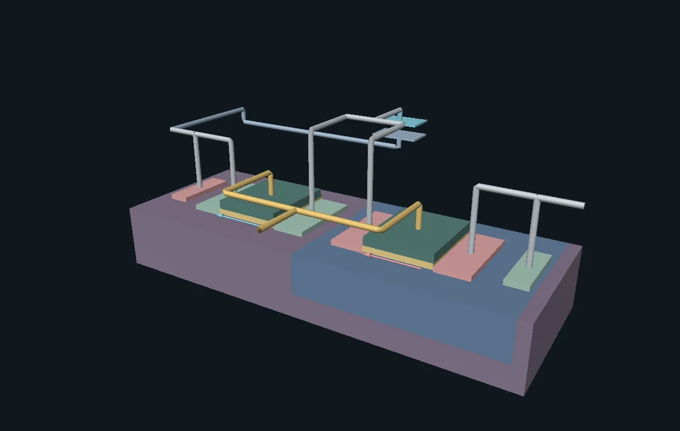 Interactive exploration
Inspect a connected CMOS cutaway, build a channel, find a circuit’s operating point and follow the charge and energy behind a changing bit.
 Interactive exploration
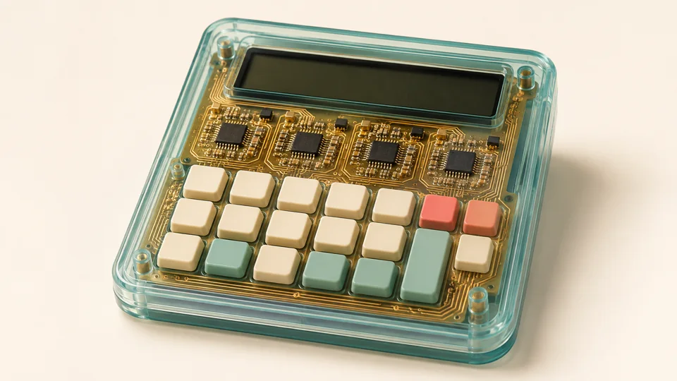
Flip real input bits on a little calculator. Build a result from simple rules, and follow a carry as it crosses four columns.
Send “SMALL IDEAS!” through a network. Delay a piece, lose another, and watch what the receiver can actually use.