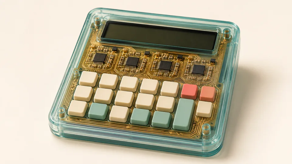
Inspect a connected CMOS cutaway, build a channel, find a circuit’s operating point and follow the charge and energy behind a changing bit.
Enable JavaScript to change the conditions and run the interactive experiment.
Make a discovery
A gate voltage changes a semiconductor channel. The circuit still needs a source of energy, a voltage difference and time to move charge. Keeping those roles separate explains how a physical device becomes part of a digital decision.
- Trace gate, source, drain and body connections in an original classic planar CMOS architecture.
- Separate an insulated gate’s control role from the output’s supply-energy path.
- Distinguish channel formation from a net drain current.
- Interpret cutoff, triode and saturation within a declared long-channel model.
- Find an output constrained by a transistor and a resistor rather than assigning it independently.
- Keep an interval-valued ideal DC result distinct from one transient voltage.
- Compare output load and input waveform using an explicit timing and energy record.
- Read threshold, resistance, capacitance and leakage specifications with their stated test conditions.
Make a prediction
At exact matched balance, Ip=In=1.125 mA. What happens to a capacitor already inside the DC interval?
- It charges at 2.25 mA
- Its voltage stays fixed while the circuit produces heat
- No current flows anywhere
Read the explanation
Net capacitor current is Ip−In=0, but the 5 V supply still delivers 5.625 mW through the branches.
Understand it
Find the insulator first
The conducting gate sits above a dielectric. Changing gate bias changes local electrostatics and the inversion layer near the semiconductor surface. It does not mechanically open a trench or feed the output current through the oxide.
Separate the material regions
This original classic planar model shows n+ source/drain in a p-type body, and p+ source/drain in an n-well. A separate body tap connects nMOS bulk to ground, while the n-well tap connects pMOS body to the supply.
Give the channel a drive
At VGS=3 V, the model supports an inversion channel. Set VDS=0: net DC current is zero. Increase VDS and the current changes, even though the gate setting stayed the same.
Find an operating point
In a resistor circuit, transistor current must match resistor current. The output is the intersection of their constraints. Moving an arbitrary marker shows a mismatch rather than creating a new valid DC solution.
Use complementary roles
With a low input, pMOS supports charging the output from the positive supply. With a high input, nMOS supports discharge to ground. The two drains share the output, while both insulated gates share the input.
Keep a special balance honest
At one exact input, the ideal flat saturation laws admit a range of DC outputs. Equal branch currents can produce zero net charging while still drawing supply current and producing heat.
Follow a finite capacitor
A prescribed input step can happen instantly in this model, but the finite output capacitance preserves output-voltage continuity. Current changes its charge over time. A bigger load requires a new initial energy account.
Compare with actual specifications
The linked named-device datasheet has different device structure and test conditions. It helps teach careful reading; it does not calibrate this fictional planar CMOS model.
Look closer at the science
Doping is not bulk net charge
p-type and n-type identify semiconductor doping and majority-carrier roles. The bulk is approximately neutral. A p-type block is not simply a positively charged solid.
The chosen gate stack
This classic planar drawing uses a conducting doped-polysilicon gate separated from silicon by a silicon-dioxide dielectric. Layer thickness, inversion shading and contact sizes are enlarged teaching choices, not a fabrication-node model.
Four terminals and voltage differences
nMOS uses gate, source, drain and body terminals. In the selected model body is tied to source. VGS and VDS matter: translating all terminals by the same voltage preserves current. Changing source alone changes those differences.
A bounded square-law model
Let u=VGS−VT. Current is zero for u≤0; β(uVDS−VDS²/2) for 0≤VDS<u; and βu²/2 for VDS≥u. The teaching values are VT=1 V and βn=1 mA/V². β includes mobility, oxide capacitance per area and a geometry ratio; no physical width or length is inferred.
Pinch-off is not an open circuit
The ideal saturation branch has finite current independent of further VDS. It is not cutoff and not a perfect low-resistance closed switch. Extra drain voltage and the high-field drain-end region are outside the displayed limiting channel profile.
A charge proxy with a common reference
The channel profile follows the same gradual-channel model. Its plotted magnitude divides the local sheet-charge factor by a fixed 4 V reference, so changing overdrive does not get hidden by renormalizing each curve to itself. Cox is unspecified, so carriers per area are not reported.
Conventional current and carriers
nMOS conventional current goes drain to source; electron drift has the opposite direction. pMOS conventional current goes source to drain. The drawn arrows identify direction, not individual trajectories or measured carrier speed.
Load-line constraint
With a positive resistor to VDD, solve ID(Vin,Vout)=(VDD−Vout)/R. Vout is a result, not a second independent supply setting. Supply power equals resistor heat plus channel heat in the DC account.
Complementary source references
For pMOS use VSG=5−Vin and VSD=5−Vout with positive current magnitude from supply to output. Passing a negative gate-source voltage into the nMOS cutoff formula would wrongly turn this device off.
Matched strength, not identical mobility
βp/βn controls abstract relative drive strength. Equal β does not imply equal electron/hole mobility or equal geometry. Moving this parameter does not establish a new measured carrier density.
The DC solution can be a set
For matched strengths at Vin=2.5 V, any Vout in [1.5,3.5] V balances the ideal branch currents at 1.125 mA each. With strength ratio b, the balance input is [4√b+1]/[1+√b] and the interval is [VM−1,VM+1]. A solver selecting one point does not make it a unique prediction.
Output charge and power
For the lumped load, CL dVout/dt=Ip−In and EC=CL Vout²/2. Instantaneous VDD Ip equals nMOS heat power plus pMOS heat power plus dEC/dt. Zero net capacitor current can coexist with nonzero through-current and heat.
An explicit transient record
The model solves one input step, linear ramp or exact-balance hold over 50 ns. It integrates output voltage, both heats, supply energy and supplied charge. Waveform corners are respected, rail violations are reported rather than concealed, and inspecting a time reads the same solved experiment.
Delay needs a reference event
Output 50% elapsed time is measured from the start of the input edge. Propagation delay here subtracts the input’s own 50% time. For a finite ramp these numbers differ. If a record does not reach the threshold, no crossing time is invented.
Changing capacitance starts a new experiment
At the same voltage, a new capacitance changes stored charge and energy. Therefore changing CL resets the transient and its ledger. For matched abrupt steps, doubling CL doubles this model’s delay and completed cycle energy.
A completed ideal cycle
Charging a 10 pF output from 0 to 5 V draws 250 pJ, stores 125 pJ and dissipates 125 pJ in pMOS. Discharge dissipates the stored energy in nMOS. At one million complete charge/discharge cycles per second this contribution is 0.25 mW; it is not total chip power.
Gate charging has its own ledger
A separate ideal 10 kΩ–100 pF gate RC example has a 1 μs time constant. Gate-wire current charges an insulated electrode, while ideal DC oxide conduction is absent. Input-driver energy and gate-network capacitances are not included in the output-node experiment.
Read the complete specification
Threshold identifies a test current and bias. It does not promise the on-resistance measured at a different gate voltage and current. Ciss is bias-dependent measured input capacitance, not a universal output load. Real leakage also differs from the model’s ideal zero endpoint currents.
Sources and model limits
- Fictional classic planar bulk-silicon n-well CMOS, not a current commercial process, microscopy image or manufacturer CAD. Layers are enlarged; overlying dielectric/passivation is omitted for inspection.
- Fixed 5 V supply, 1 V threshold magnitude, constant mobility, α=1 and λ=0. Body tied to source is a separate assumption from α=1. No subthreshold/gate leakage, channel-length modulation, body effect, velocity saturation, temperature dependence, DIBL, breakdown or junction conduction.
- Only positive source-referenced device biases and inverter outputs on the stated rails are modeled. No reverse-bias/body-diode or arbitrary terminal-excursion model.
- Channel shading is a normalized sheet-charge proxy, not counted electrons, carriers per area or a measured flow speed. The limiting saturation profile does not resolve the drain-end high-field region.
- The 50 ns output-capacitor record omits input-driver energy and gate-network capacitances. The separate lumped gate RC comparison must not be added silently to that ledger. Large loads may not settle before the record ends.
- The ideal DC balance interval does not predict a real metastability lifetime or reliable analog memory. Source reading and independent numerical checks do not replace a validated compact device model.
- NIST’s unchanged illustration concerns defect trapping/noise, which is omitted here. The 2N7002 trench-device datasheet is a conditions-reading comparison, not a fitted parameter source.
- Paper cards encode quantities and topology. No powered device, heating, soldering or physical semiconductor measurement is required. Subject review, learner trials and device/export checks remain release gates.
Long-channel current, channel profile and model limitations
MIT 6.012 Lecture 11, MOSFET current derivation and gradual-channel assumptions. Product geometry is original; lecture figures are not redistributed.
MIT 6.012 · MOSFET current modelComplementary inverter, transfer and load energy
MIT 6.012 Lecture 14, circuit/transfer characteristic and slides 20–24. Toy timing values are independently computed, not commercial specifications.
MIT 6.012 · CMOS inverterClassic planar n-well topology and body contacts
Author-hosted CMOS VLSI Design chapter 1, section 1.5, Figure 1.34 page 20. Used as a topology reference; no book artwork copied.
Weste and Harris · CMOS VLSI DesignReal gate charging and driver limitations
TI SLUA618A, sections 2.4–2.7. Real power-switch driving differs from this ideal output-capacitance experiment.
Texas Instruments · Gate driver fundamentalsNamed device specifications with test conditions
2N7002 Rev. 7, Table 7, page 5. N-channel trench MOSFET, not the modeled planar device. No datasheet figures redistributed.
Nexperia · 2N7002 datasheetExact source illustration identity
NIST image record labels the visual an illustration. Original 1429×883 source retains its full defect-trapping annotation and exact hash.
NIST · MOSFET illustrationDefect trapping and random telegraph noise
NIST research account published 7 November 2017, updated 17 March 2025. This effect is an explicitly omitted-physics comparison.
NIST · Captured electrons and flash memorySource image reuse basis
NIST permits copying and distributing site information except marked copyrighted material and requests attribution. No image-specific third-party mark was found. This is not an invented CC0 license.
NIST · Copyrights and disclaimersIndependent subject review is pending.